Analog Battery Management System
About 6 weeks ago I read a blog post by Vlastimil Slinták in which he attempted to develop an Analog Battery Management System (BMS) for a 1s3p Lithium Titanate (LTO) battery pack. From what I understand, he ended up running into an issue where he could not drive a PMOS’s gate high enough to open it fully, and decided to go with a low-power microcontroller in the end.
I took some time to understand the circuit and decided it would be a good exercise to learn more about analog electronics and PCB design. A microcontroller really is the best way to build a BMS, but analog circuitry is fun to learn about and how our forefathers did things.
Fundamentally, a BMS has 5 main functions:
- Undervoltage protection (UV)
- Overvoltage protection (OV)
- Undertemperature protection (UT)
- Overtemperature protection (OT)
- Overcurrent protection (OC)
Other functions include cell balancing, state of charge (SoC) estimation, and communication with other devices. These were out of scope for an Analog BMS and I get a good enough taste of these technical problems on the UBC Solar student design team where I work on the BMS for our 5.4 kWh Li-ion battery pack.
See all my project notes, BOM, testing data, and KiCAD / Solidworks files on GitHub.
Schematic Overview
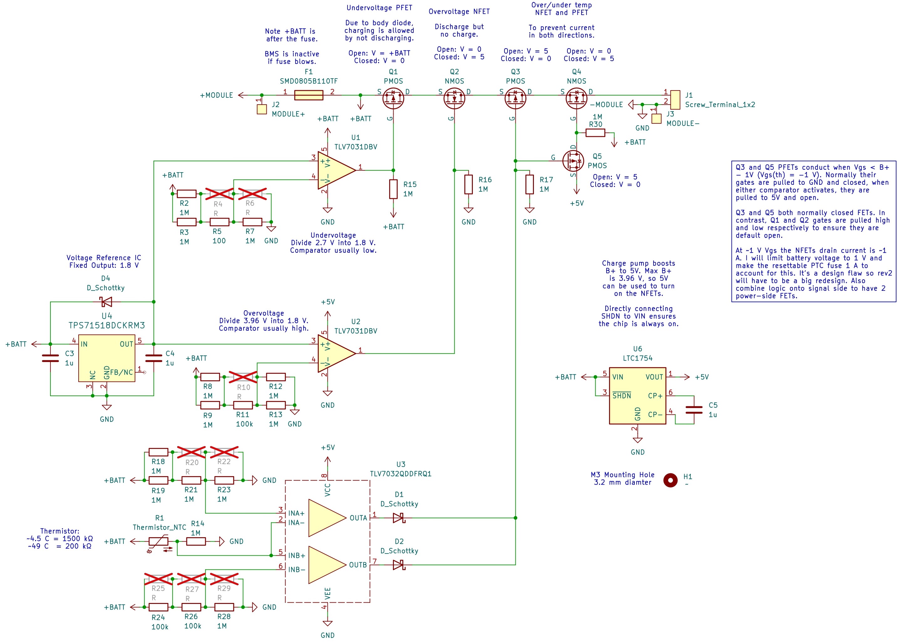
MOSFET Body Diodes
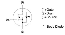
Notice the intrinsic body diode of this NFET points from source to drain. Current can always flow from source to drain if Vs - Vd > Vth.
The fundamental principle of this BMS is leveraging the intrinsic body diodes of MOSFETs to toggle current flow in a given direction, but always allow current to flow in the opposite direction. Doubling up on FETs antiparallel to each other (eg. drain to drain) is a common technique to prevent current flow in either direction when both FETs are off.
For undervoltage (UV) protection, I used a P-channel MOSFET (PMOS) with source to BATT+ and drain to the load. When the gate is pulled to GND, this FET conducts and current can flow out of the cells. When the gate is pulled to BATT+, the FET is not conducting and current cannot flow out of the cells. However, current can still flow into the cells through the body diode of the PMOS. This allows us to charge the battery when the voltage is critically low, but not to discharge.
A similar arrangement is used for the overvoltage (OV) protection, however I used an N-channel MOSFET (NMOS) instead. If I used a PMOS, I would have to pull the gate voltage below 0 V (Source voltage to load, 0 V initially) for it to be conducting. With an NMOS, I need to pull the gate voltage above BATT+ for it to be conducting. This meant I either needed a charge pump outputting a negative voltage, or a way to source a voltage higher than BATT+. I followed Vlastimil’s original design and used a charge pump to get ~5 V, a boost converter would have also worked and may have been a better choice to get a more constant voltage.
Toggling UV/OV Fault Conditions
To detect undervoltage and overvoltage conditions, I used two comparators (TLV7031) that compared divided battery voltages to a fixed 1.8 V voltage reference. These comparators were chosen for low quiescent current, rail-to-rail operation, and fairly high hysteresis (10 mV typical).
I baselined the use of Molicel’s INR-18650-M35A cells, which are the cells that UBC Solar uses. This provided a voltage range of 2.7 V to 4.2 V per cell, giving me my UV and OV conditions.
To simplify the BOM, I used a single 1.8 V fixed voltage reference (TPS71518) and two voltage dividers to scale the battery voltage to toggle the comparators at the desired voltages. For example, for undervoltage I divided the 2.7 V minimum voltage of the cells into 1.8 V and connected this to the inverting input of the comparator. The non-inverting input was connected to the 1.8 V reference. When the battery voltage dropped below 2.7 V, the output of the comparator went high, pulling the gate of the PMOS to BATT+ and disabling discharge.
My original design involved two voltage references (TPS7A2401) that would output 2.542 V and 4.142 V. These values were the closest I could trim the output of the references to 2.5 V and 4.2 V (I hadn’t yet realized 2.7 V is the correct value for UV for battery chemistry reasons). Chris Jack (Great name) pointed out that I could get away with a single 1.8 V reference and two voltage dividers, instead of 2 references and 2 dividers.
I ended up having issues with the voltage dividers not dividing BATT+ properly because of the extremely weak resistors (~1M to limit quiescent current), so this was an incorrect design decision I didn’t explore far enough (more on this later). A common theme in this project was making poor design decisions because of a lack of theoretical understanding.
Temperature Faults
Temperature faulting circuitry uses the same principle as the UV/OV circuitry with FETs and comparators. The difference is that I used a 560k NTC thermistor and an additional PMOS.
To sense temperature, I hooked up the NTC thermistor in a voltage divider with a 1M resistor from Batt+ to GND. This way, voltage at the midpoint of the divider increases as temperature increases. By referencing this against voltage dividers from BATT+ to GND, I could toggle comparators at given temperatures.
I set up the comparators to output high (5 V) whenever a fault temperature occurred. Because I used a rail-to-rail comparator (TLV7032) and the comparator outputs are connected to each other, I added a diode in series with each output to prevent one comparator outputting high and the other low (eg. one OT and other nominal) and effectively shorting GND to 5 V. This is a good time to mention that if you have any better ideas for this circuitry please email (christopher.kalitin@gmail.com) or DM me.
The UT/OT comparators output high during a fault condition, which is what’s required to open the PMOS. However, the NMOS needs to be pulled to GND to open, so I added a PMOS with source to 5V, drain to the gate of the NMOS, and gate to the output of the UT/OT comparators. This way, I flip the logic of the UT/OT comparators to drive the NMOS gate low during a fault condition.
Don’t Do Logic Power-Side
As one of my Moots pointed out, a mistake in this design is doing UT/OT logic power-side instead of signal-side. All MOSFETs have an on resistance (Rds(on)), and a BMS should aim for as low resistance as possible to minimize power loss. By adding 2 more FETs in series with the load path, I increased the overall Rds(on) of the BMS. A better design would be to do all OT/UT logic signal-side, so as to not add more resistance power-side.
He also pointed out that the drain current of NMOS’s is a function of Vgs, and with only 0.8 V between my NMOS gate and source when the battery is at 4.2 V, the drain current is ~100 mA. I decreased the OV threshold to 4 V to increase the max current to ~1 A. This is a bandaid on the problem and is a result of a fundamentally flawed design, but it works for a learning exercise PCB.
Breadboarding Temperature Circuitry
To confirm the temperature circuitry I designed worked, I breadboarded it up and tested it by shorting the equivalent of the thermistor voltage divider output to PSU+ (OT fault) and GND (UT fault). This worked first try!
Quiescent Current & Part Selection
The primary consideration I took into account for part selection is ensuring all components had low quiescent current. The BMS is always connected to the battery, so it must draw a very small amount of current to avoid draining the battery over time, and potentially going low enough to damage the cells.
Two of the 18650 cells I chose have a capacity of 7000 mAh. If the BMS draws 50 uA (Vlastimil Slinták got 50 uA), this would drain the battery in 140,000 hours, or 16 years. This is acceptable for a BMS.
The full BOM is available here and all notes about part selection are in my project notes.
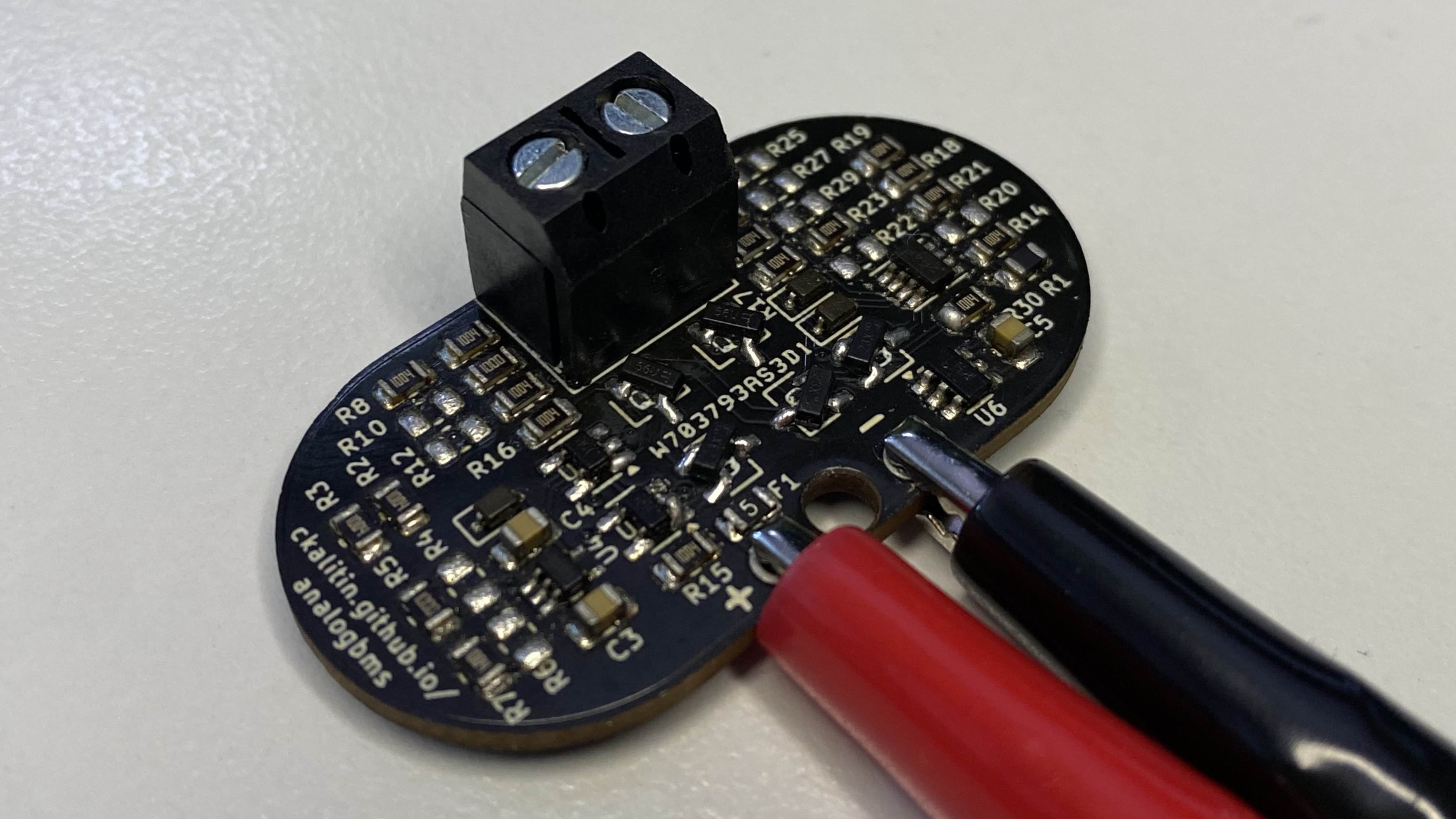
PCB Routing
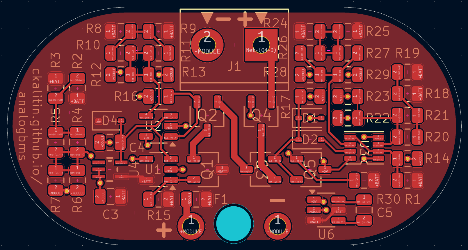
Ari Wasch pointed out that direct connections would be ideal instead of thermal reliefs for the high current paths. I set the entire top layer of the PCB (BATT+) to use direct connections instead of thermal reliefs and didn’t really have any problems with this. Resistance was marginally decreased and I never had issues soldering / desoldering components.
I asked former UBC Solar Electrical Lead Mischa Johal about if we have / should use direct connections on our module sheet PCBs (they hold and provide current paths for our cells) to decrease the resistance of our pack. Apparently some characterization testing was done on this (with little documentation) and it was found that temperatures didn’t significantly increase and resistance didn’t significantly decrease.
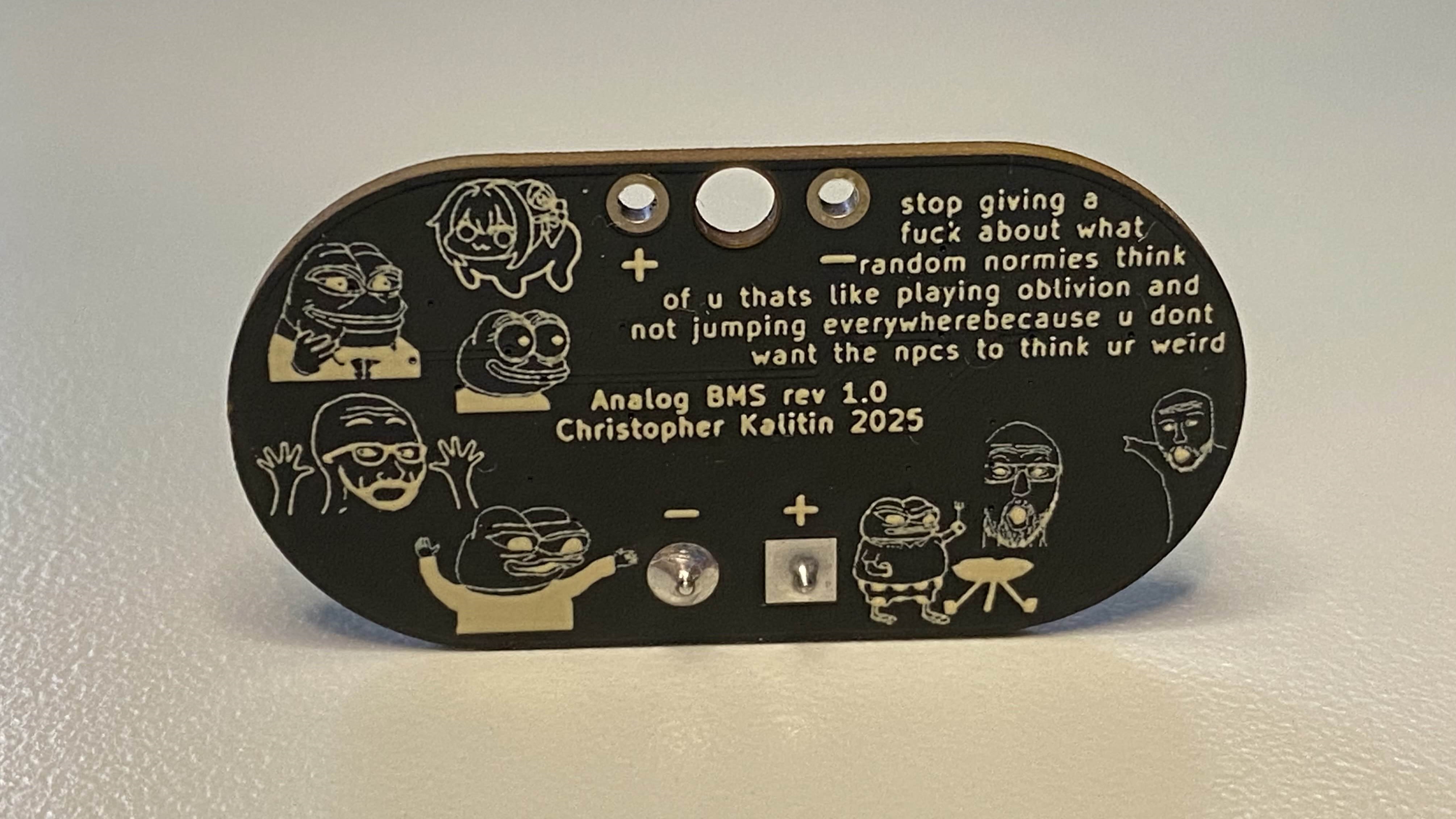
Expanded Image. I love my moots.
One of my moots gave the amazing suggestion of removing all reference designators and replacing it with fun squiggles. The only logical response to this is to get all my moots to send me their best pepes and memes to put on the PCB, along with my favourite 4chan greentext.
Enclosure Rev 1
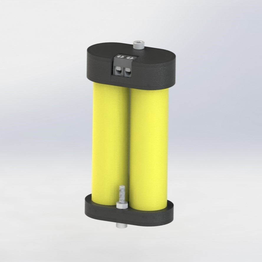
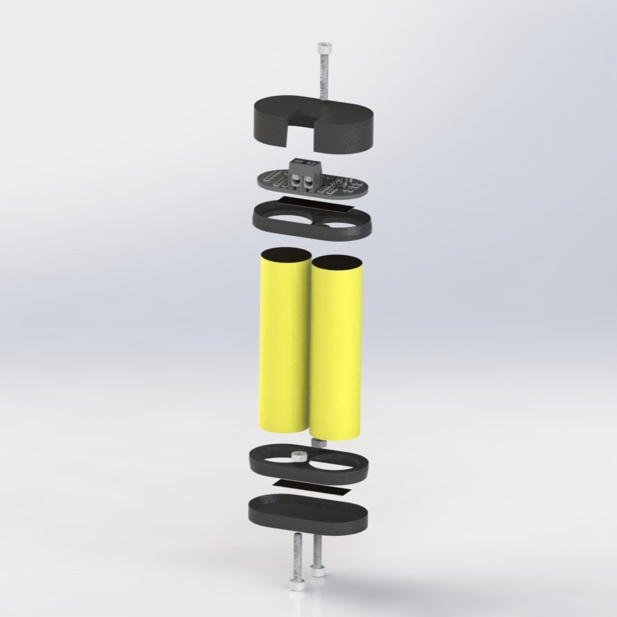
After the PCB was completed, I took a first run at designing an enclosure for the battery module using Solidworks.
My first attempt required 3d printed parts on the top and bottom of the cells to be installed before nickel tabs were spot welded to the cells (allowing for no repairability) and 3 screws to hold the outermost parts of the enclosure to the inner 3d printed parts. Suboptimal design.
Because there’s a screw terminal on one end of the PCB, there’s only a single screw holding the PCB in place, which allows for rotation on the vertical axis.
To connect the bottom of the cells (Batt+) to the PCB, I would have used a 16 gauge wire soldered to the PCB and to the nickel tab on the bottom.
Finally, the bottom of the PCB would be directly above the top nickel tab (Batt-), and any through-hole components (eg. for the positive and negative terminals of the screw terminal) would be at risk of shorting to the nickel tab (most critical failure mode of a battery).
This is all to say that my first iteration is a terrible design. It’s a far better idea to make everything a snap-fit to the cells, consider using cells with both terminals on the same side like Vlastimil did, and to better isolate the PCB from the top nickel tab.
PCB Bringup
PCBWay offered to manufacture a PCB of mine for free if I made a review of their product.
The PCB is obviously functional and looks very beautiful. The silkscreen doesn’t have the highest resolution, but this is a function of me using very small text. They threw in a free stencil as well, the nice kind that’s as big as a picture frame. They did only give enough credits to get the slowest shipping option for free, so they saved ~$5 on shipping on my behalf at the expense of 1.5 weeks.
PCBWay is obviously one of the big PCB manufacturers so the product is as expected. The differentiating factor is they do give you free PCBs if you ask!!! That’s a very important differentiating factor.
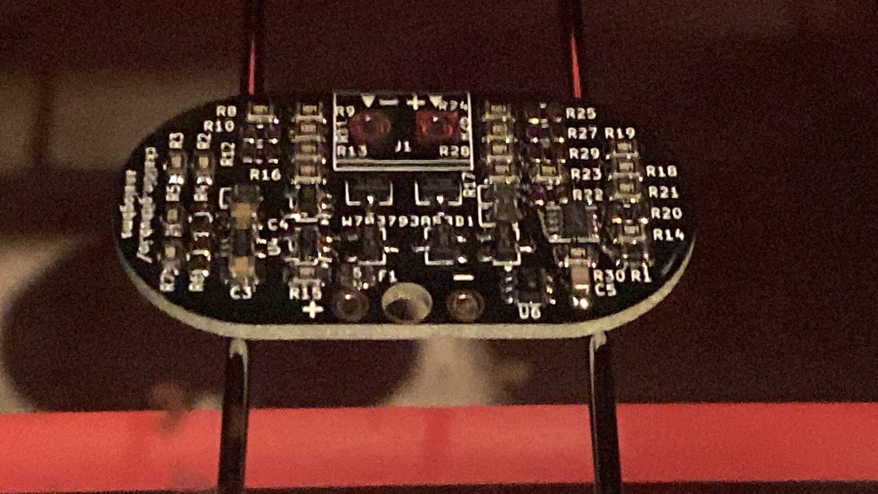
I used the reflow oven I made a couple of weeks ago on this PCB. This was the first time I used the reflow oven on a real project and it worked great.
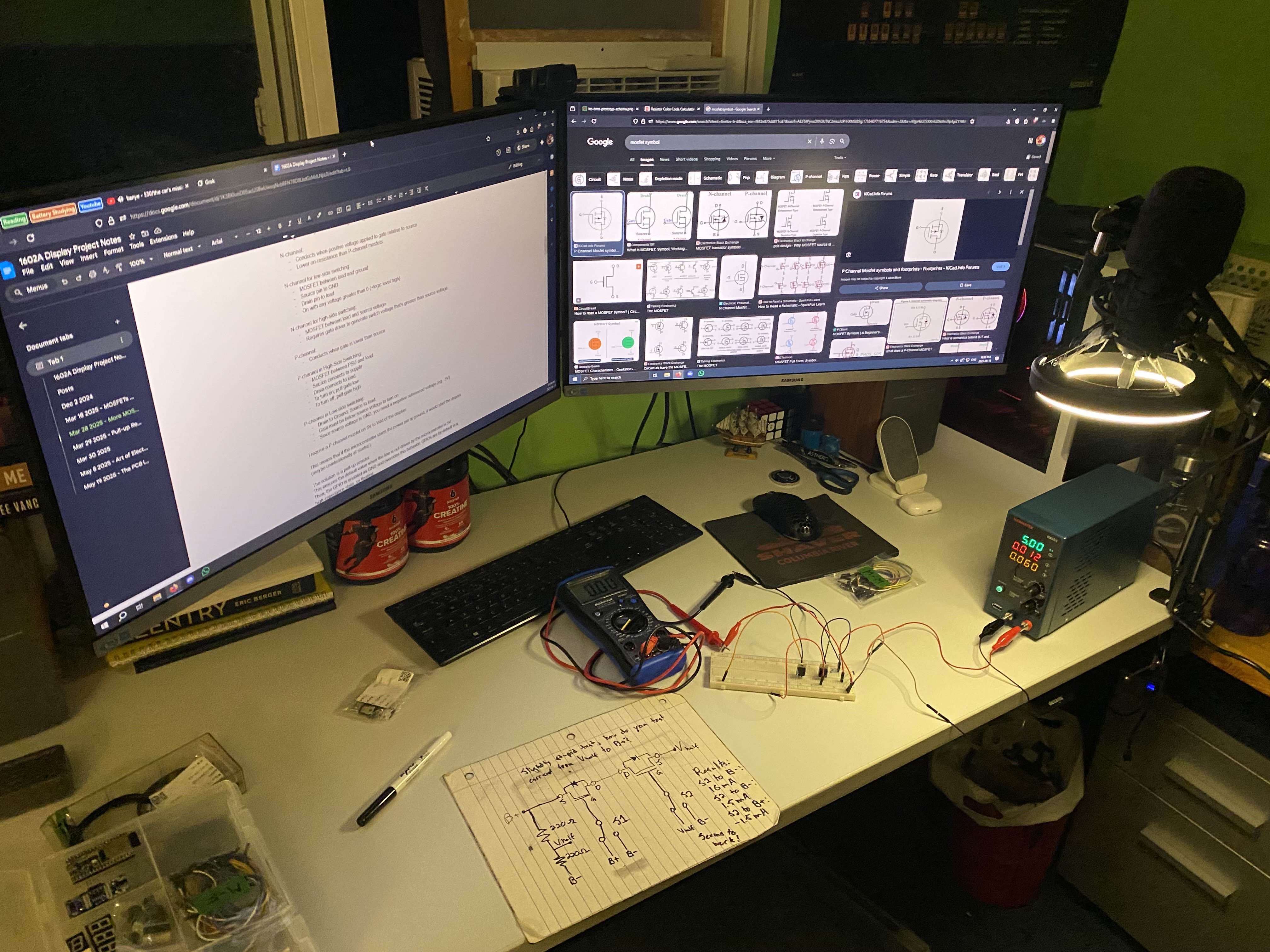
Debugging
I ran into a painful amount of issues during testing and easily spent many multiples more time debugging than designing. A good lesson to have forced into your head is that you can spend a little more design time to prevent debugging or make debugging easier later and you’ll probably be saving time on net.
Below is a list of a few issues I encountered, a lot more of them are described in a more inscrutable manner in my project notes.
Incorrect Resistors
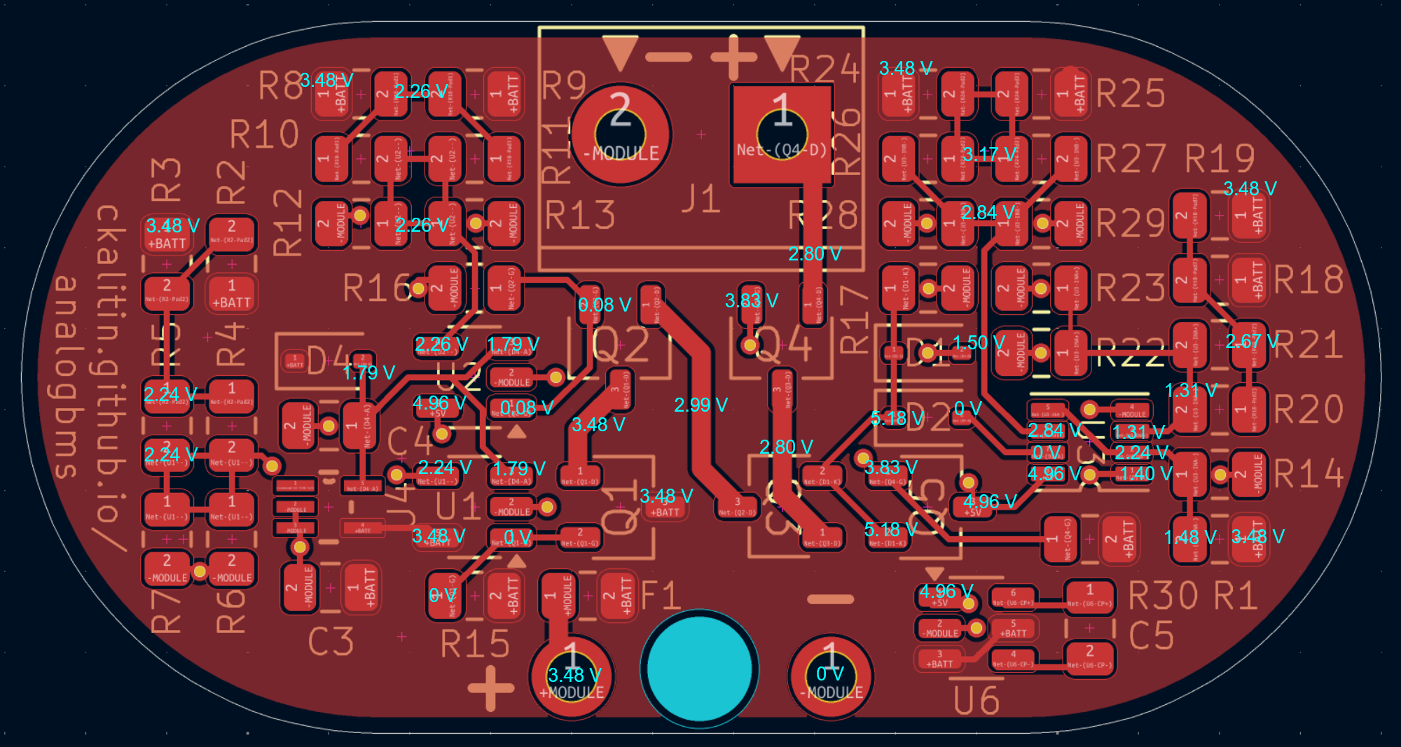
Expanded Image. Annotated trace voltages test data in firefox. All available in the Git repo.
First, a fairly mundane issue. In my project notes I came to the conclusion that for the overvoltage BATT+ voltage divider I would need to use 600k and 500k equivalent resistances for the top and bottom of the divider respectively. I noted this down but never updated the schematic so manufactured the PCB with incorrect resistors.
When I encountered behaviour that didn’t align with my expectations at all I started annotating PDFs of the schematic in firefox and added text boxes with observed voltages for all relevant traces. This is how I found the OV voltage divider was incorrect.
Incorrect MOSFET Footprint
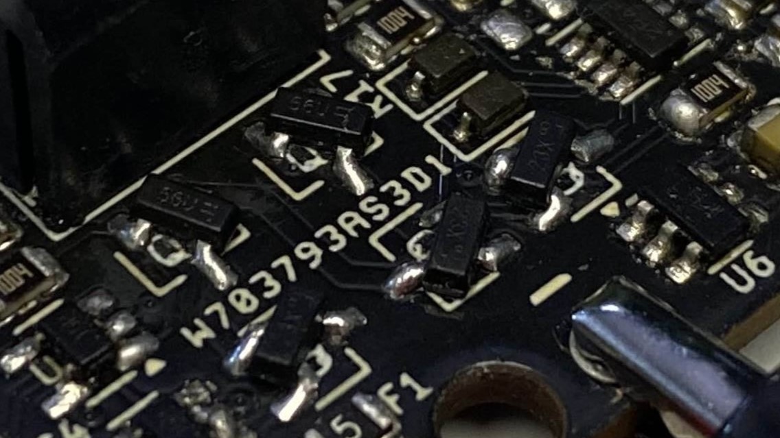
Labelling trace voltages also helped me to figure out that all my MOSFET footprints were incorrect. I used the built-in KiCAD libraries for MOSFET schematic symbols and footprints, and these are not consistent with each other. SOT-23 is not purely used for MOSFETs, so the pinout is not consistent.
Luckily, SOT-23 FETs are mostly symmetrical at 120 degree rotations, so I was able to desolder and rotate all FETs 120 degrees to get the correct pinout.
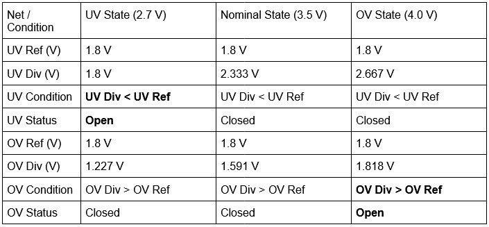
This table defines expected voltages and FET states for given BATT+ voltages. Screenshot from project notes.
While attempting to figure out the issues with the OV voltage divider and FETs, I made a truth table of expected voltages and UV/OV FET states for given BATT+ voltages. This way I had a very clear visualization of what should be happening for given BATT+ voltages and I could easily compare to observed behaviour.
For all analog comparator / logic circuitry you should always make a truth table like this so you’re never guessing or trying to remember what should be happening.
Weak Temperature FET Pulldown
Several times during testing I found that the UT/OT FETs were not conducting or did not have the state I expected them to. When I probed the gates of these FETs, I found that they were ~3 V instead of 0 V or 5 V. This meant the gate of the FETs were not being pulled to a definitive state, or maybe the FETs themselves were damaged. When I soldered a 1k leaded resistor over the pads of the R17 pulldown resistor, the gates were pulled down to ~0 V as expected. They didn’t get quite down to 0 V (eg. 50 mV), so there is likely still some issue with the comparators / FETs.
Inconsistent Voltage Dividers
Expanded Image. LTspice sim available in the Git repo.
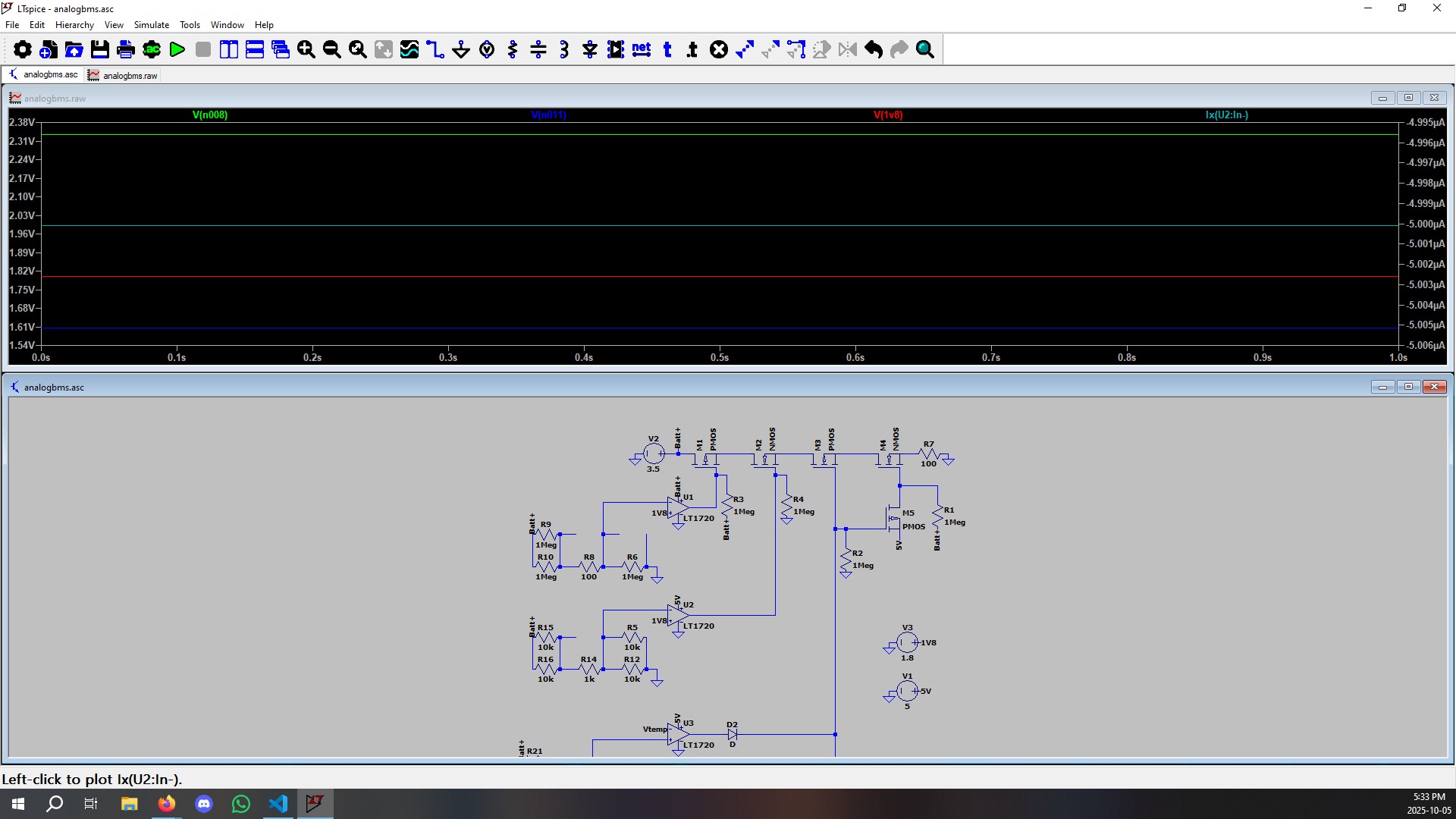
As part of creating a truth table of expected behaviour, I learned the basics of LTspice and simulated the entire BMS circuit. LTspice’s comparator model backfed current into the voltage dividers for UV and OV because the dividers were too weak (1M resistors). This meant that the voltage at the comparator inputs was not what I expected, and the comparators were not toggling when I expected them to.
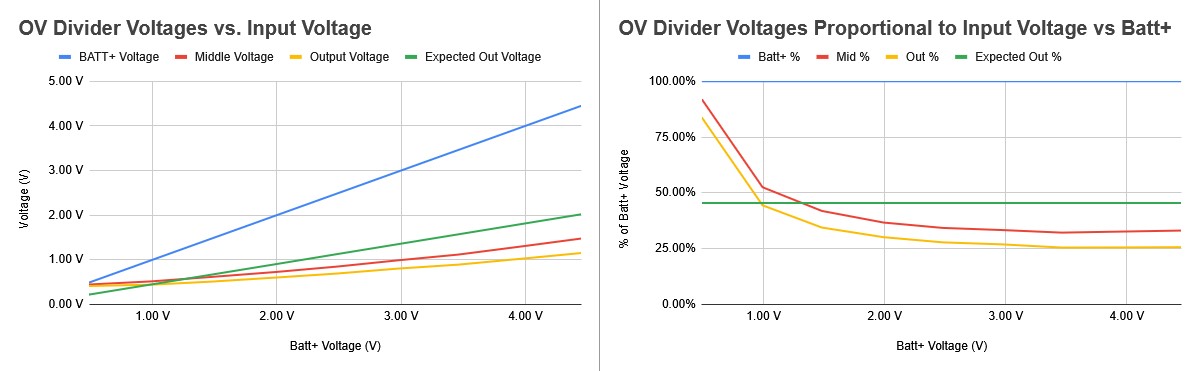
Expanded Image. When plotting the OV voltage divider output for given input voltages, I did not get a linear response.
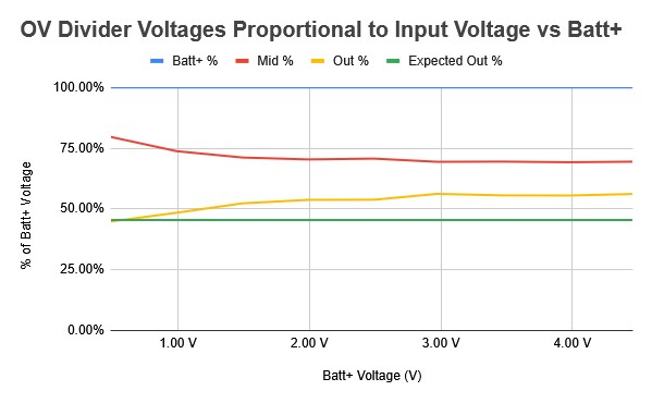
Expanded Image. After replacing the comparator and using 5k/10k voltage divider (instead of 500k/1M), I got a linear response.
The result of the LTspice sim was not what I expected, but I didn’t see any issues with the PCB at the time that I made the sim. However, later when I tested the OV voltage divider output as a function of BATT+ voltage, the output was very non-linear and clearly the comparator was causing some issues.
This issue goes back to my decision to use a single 1.8 V reference, instead of 2 voltage references. If I used 2 voltage references, no unexpected current would be going through the voltage dividers and the references would be outputting the correct voltages. Fundamentally, this is due to a lack of theoretical understanding of comparators on my part. I haven’t gotten that far in Elec 204 at UBC or in Practical Electronics For Inventors or The Art Of Electronics.
I replaced the comparator and used stronger 5k and 10k resistors for the divider and got a mostly linear response (the inconsistency in the graph above is due to low resolution of my multimeter and high % error at low voltages (since voltage measurements have constant precision, you get greater % error at low voltages)).
These stronger resistors draw more current (I=V/R, so 4.2 V / 10k = 0.42 mA), which is unacceptable for a BMS but not for a learning exercise PCB. I should have done more breadboarding and LTspice simulating before manufacturing the PCB to avoid this issue.
I’m Calling The Project Complete
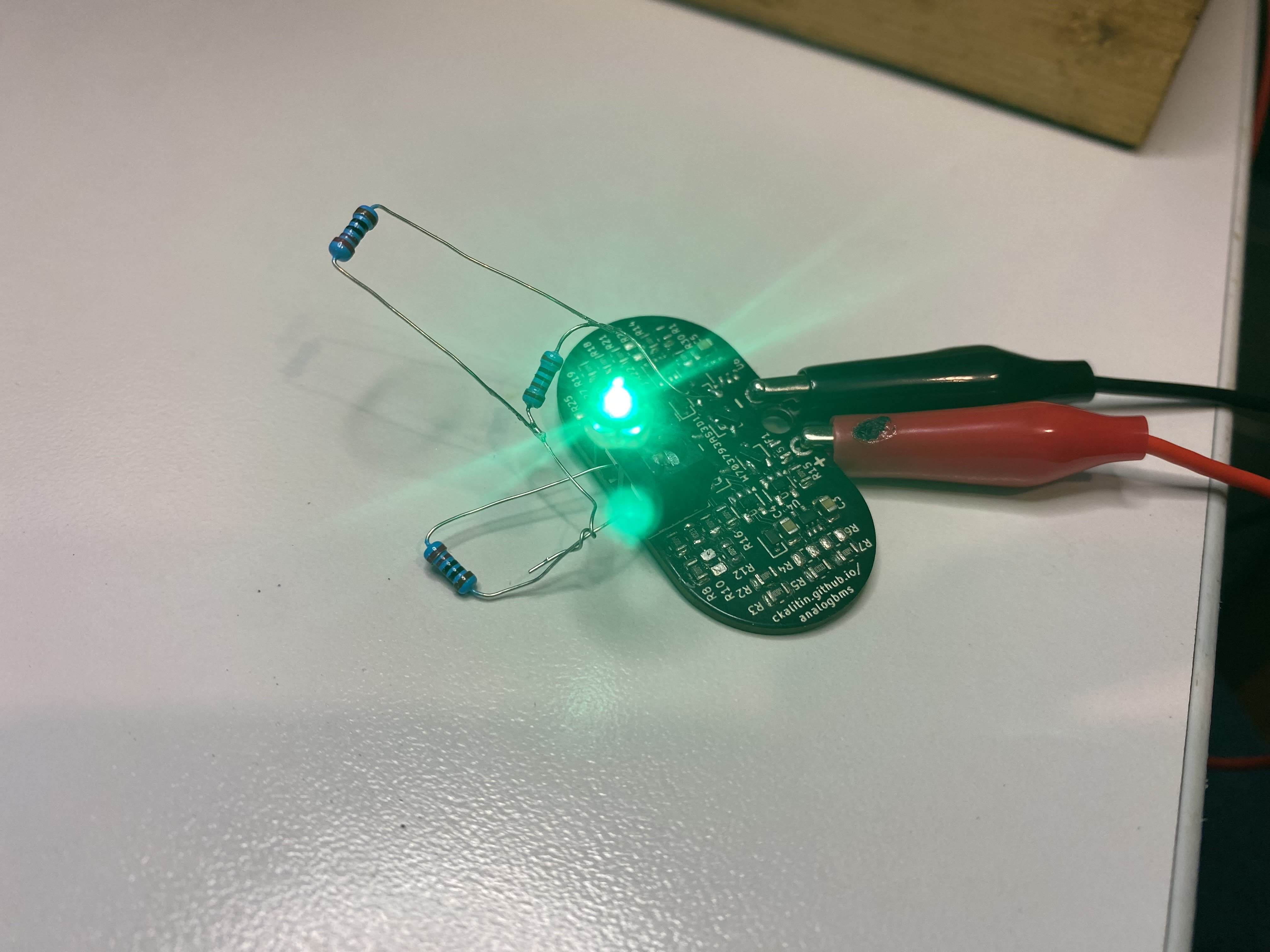
In the end, I was able to pull current out of the BMS PCB when simulating the cells with a power supply. Great success! That LED actually turned on!
I was able to validate undervoltage protection and the functionality of the over/under temperature faulting comparators. I used a PTC fuse to OC and when I shorted the output to GND with a 1 A current limit on my power supply, I read 300 mA of current. PTC fuses don’t work in the way that I expected them to, as current flow wasn’t completely cut off immediately. The temperature of the fuse did reach 37 C. Overvoltage protection I was not able to validate because of the issues with the OV voltage divider and comparator, I made a mistake not using 2 voltage reference ICs.
The clearest insight I got from this project is that I should put more effort into understanding the theory behind what I’m doing before jumping into circuit and PCB design. If I had finished the Op Amp chapter in Practical Electronics For Inventors this project would have been much more successful. This would have solved the voltage divider issue and saved me many dozens of hours debugging!
Breadboard testing also would have been a way to catch issues before I ordered the PCB. I should have done more breadboard testing than just the temperature FET circuitry. When you don’t have a 100% clear understanding of what you’re doing, breadboard the circuit and play around with it. Otherwise, if you’re in a well explored problem space, you can probably get away with not breadboarding.
This project is not quite on the critical path to Conquering the Primary Energy Layer of Civilization, so I’m calling it complete and moving onto learning about fluids systems and chemical reactors. I work on a 5.4 kWh Li-ion battery pack on UBC Solar so I’m not missing out on much by not finishing the enclosure and spot welding two cells together. Overall, I got many useful painful hours of debugging and learned a lot about what I don’t know. More exploration of the collective knowledge space of humanity is always worth it!