2nd Year Circuit Analysis Being Useful
Project Background
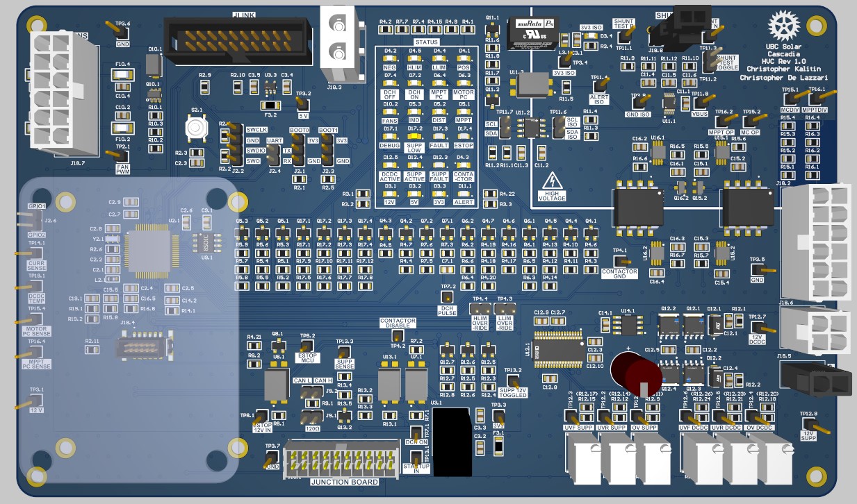
Since September (ugh, go faster) I’ve been working on the High Voltage Controller (HVC) for UBC Solar’s fourth (fifth?) solar car.
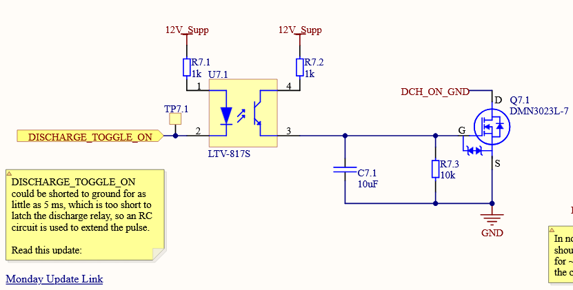
One of the functions of this board is taking in raw 12V signals from around the car as control inputs. These include ESTOP (normally 12V, active low), Startup (either GND or floating), and Motor Discharge Toggle On (either GND or floating).
Because these wires go all around the car to the driver startup switch / ESTOP buttons, we need to ensure noise isn’t an issue. With many meters of wire going all around the car, and near the motor and main pack (HVC is inside the main pack), it’s not unreasonable to expect a case in which a few volts of noise can momentarily appear on these lines. A few volts could be enough to cause a MOSFET’s gate to toggle, which could cause a dangerous situation.
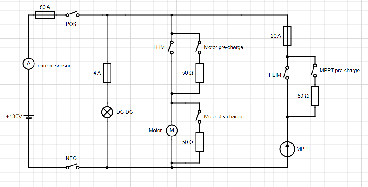
Electrical diagram of UBC Solar’s V3 Battery Pack.
For example, if we accidentally enabled motor discharge, we’d effectively be adding a 50 ohm resistor across the terminals of the pack, 134 V (max voltage) ^ 2 / 50 ohms = 360 W of power being dissipated through that resistor, while it’s rated for 50 W.
To ensure we don’t have such noise issues, we use an optocoupler to isolate the toggled signals from the rest of the HVC. I explain more in section 5.2 & 5.3 of this document.
Now you know the background. The rest of this blog post is just two copy-pasted project updates I wrote this morning for the team which show a fun example of how my 2nd year circuit analysis class (ELEC204 at UBC) has come in very useful in a practical application.
Seeing clearly how such a class is useful is always a great bit of feedback. My experience in the vast majority of classes (esp. highschool) is that they’re completely useless or even anti signals (like university tech comms classes), and this is a great example of the opposite, a class that had great practical applications after the class itself (and even during, with what it taught me about Op Amps I figured out the failure modes of my Analog BMS and why it didn’t really work!).
If you’re interested, all of my previous project updates (some mentioned here) are available in this repo.
Simulating Optocoupler DCH_ON Circuit
LTSpice sims saved in the Drive.
Problem Background

I was concerned the circuit above wouldn’t work due to R11.8, the emitter pull-down / load resistor. I simulated pretty much the same circuit shown above, where it’s very important for emitter voltage to rise high enough to close the MOSFETs.
Problem Description
As described in the previous update, I used an RC circuit to extend the pulse of DISCHARGE_GND_IN by ~10x to ensure that even a pulse as short as 2 ms will extend to be long enough to latch the discharge relay.
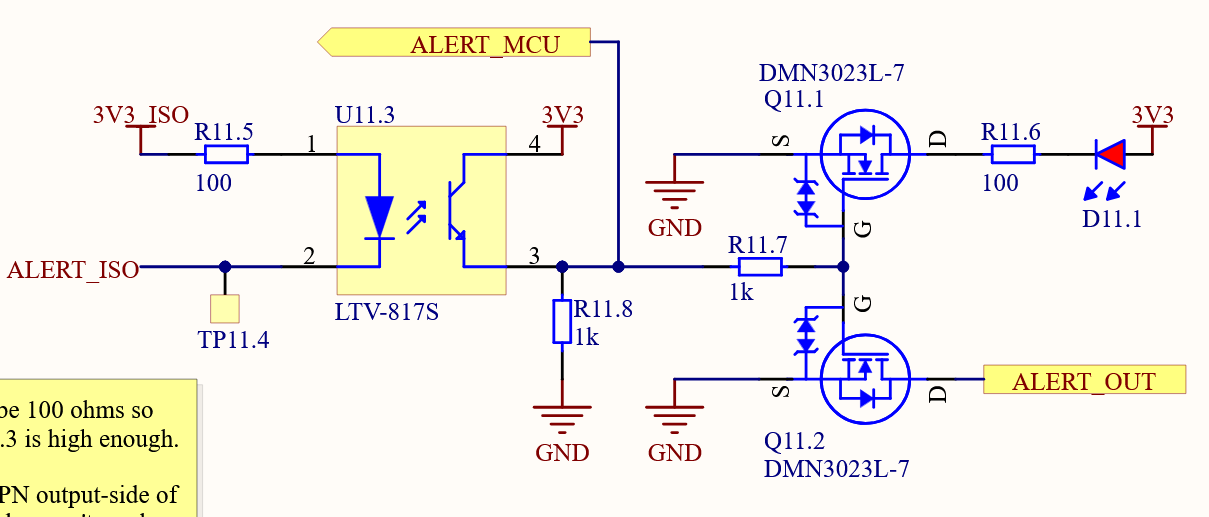
During the team-wide DR yesterday, Saman pointed out I used a few Optocoupler’s incorrectly with common collectors instead of common emitters.
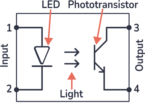
Notice in the images above that an Optocoupler contains an NPN BJT on the output-side. NPNs require V_BE > 0.7 to conduct. If, for example, the emitter was at 3.3 V and the base was at 3.3 V, then the NPN wouldn’t conduct.
For an optocoupler, base voltage is proportional to LED input voltage (Pin 1 in the first image of this update). So, if LED voltage input is 3.3 V, base will be around 3.3 V.
This could occur if the load-resistor is placed low-side (on the emitter) instead of high-side (on the collector). My LTSpice sims below show this topology.
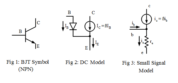
In this case, voltage will drop over the low-side resistor, meaning the emitter will be at GND + V_Resistor. There are only two places in this circuit where voltage drops, the NPN (V_CE ~= 0.2 V) and the resistor. So, the resistor will drop most of the voltage, and hence V_E ~= 3.3 V - 0.2 V = 3.1 V.
If anything is unclear, look at the circuit below and remember 2nd year circuit analysis.
Theory As To Why The Circuit Would Work
I had a theory that output voltage will converge to around V_CC - V_CE (3.3 V - 0.2 V) because the NPN wants to conduct.
Example of states:
- V_LED = 3.3 V, V_C = 3.3V, V_E = 0 V -> NPN conducts (V_BE > 0.2 V)
- V_LED = 3.3 V, V_C = 3.3 V, V_E = 3.1 V -> NPN reaches equilibrium
This however will only occur if the emitter resistor (R1 & R3 in the sim below) is of great enough resistance.
Important points:
- NPNs are current sources
- In optocouplers, their current is dependent on LED current and Current Transfer Ratio (~100% In:Out)
- V=IR
Because we’re limited in how much current can be produced, the emitter voltage is limited (V=IR, I is limited, R is a constant).
My worry was that if the ratio of the input to output resistor (LED to NPN resistor) was too small, the emitter voltage wouldn’t rise high enough to close a MOSFET (shown at the top of this update.
Simulation
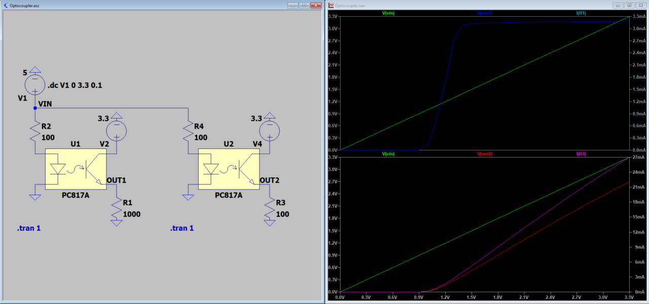
I simulated an optocoupler circuit in LTSpice and took a sweep of input voltages. The green line in both graphs is input voltage, blue/red is output voltage (emitter), and teal/pink is current through the NPN load resistor.
Above you see two cases of the circuit:
- Both have LED resistors of 100 ohms.
- The first circuit (left circuit, top graph), has an NPN load resistor of 1000 ohms.
- The second circuit (right circuit, bottom graph) has an NPN load resistor of 100 ohms.
Notice that when the NPN load resistor of 1000 ohms, the emitter voltage goes to ~3.1 V very quickly.
However, if the NPN load resistor of 100 ohms, we saturated NPN current and it only increases at LED input voltage increases. Hence, the NPN resistor is current-limiting component, instead of the resistor being the current-limiting component.
This results in emitter voltage slowly climbing, instead of quickly converging to 3.3V.
These results simply tell us that using a 100 ohm LED resistor and 1000 ohm NPN resistor is a valid circuit to get output voltage (at the emitter) high enough for our purposes.
Hence, the circuit I showed at the beginning will work:
Note:
Yesterday R11.5 was a 1k resistor, which wouldn’t have worked! Very good that Saman scrutinized my design days before ordering!
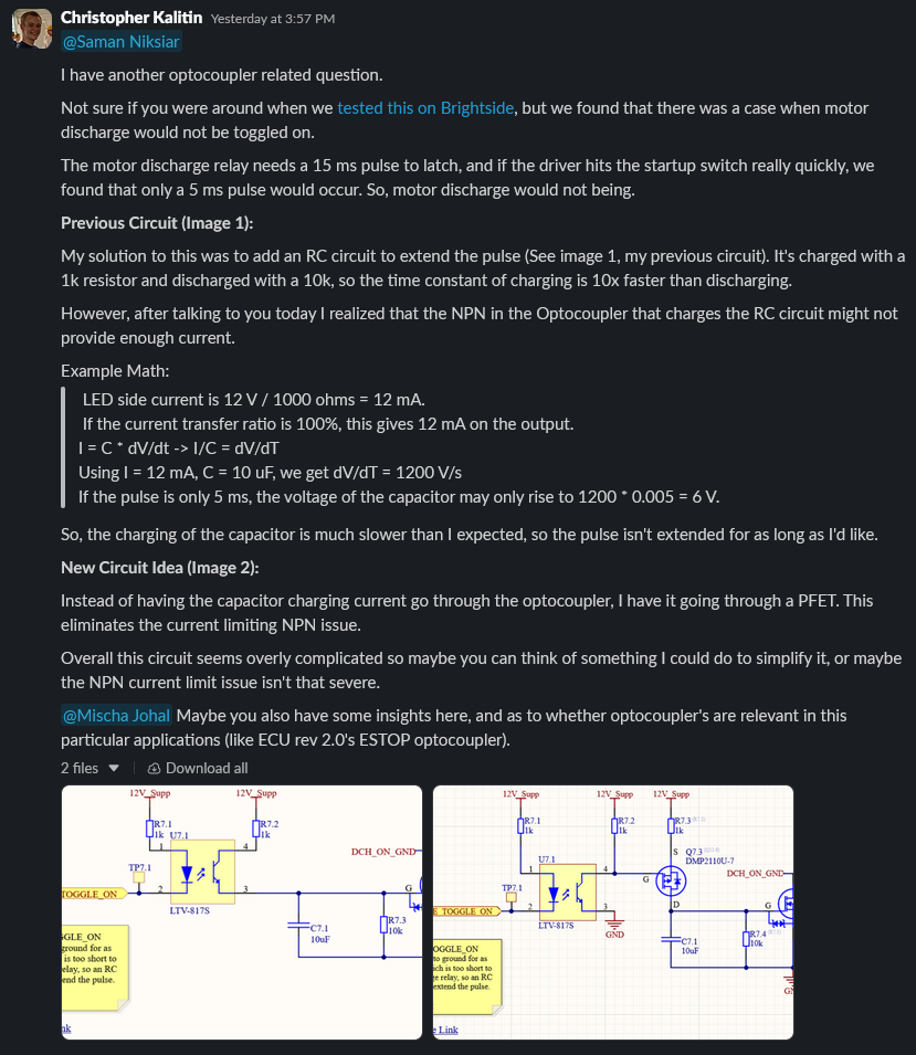
Christopher Kalitin (11h)
My original question to Saman:
Simulating Optocoupler Discharge Pulse Extension Circuitry
Similar to the previous Optocoupler update this morning.
LTSpice sims are on the drive.
Conclusion:
- Use a 1uF instead of a 10uF for RC circuit (and change 10k to 100k to keep time constant the same)
- Use ~500 ohms on optocoupler input
- This makes the charging time constant 100x lower than the discharge time constant, for optimal pulse extension
The Concern
As explained in the previous update, I was concerned about the NPN BJT in the optocouplers being limiting the current in some circuits.
In the case of the RC pulse extender circuit, this could mean not charging the capacitor fast enough, meaning the charging pulse is artificially shortened. In a worst case, this means not latching the discharge relay.
I decided to simulate the circuit in LTSpice to confirm functionality.
Simulation 1
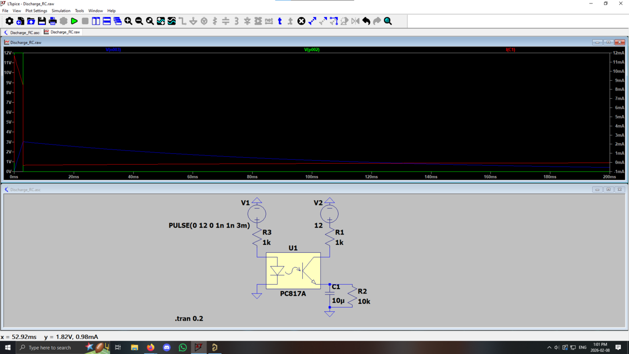
Parameters:
- Input Pulse: 3 ms
- RC Capacitor: 10 uF
- Input Resistor: 1k
This simulation is a worst-cast scenario for the RC pulse extender circuit with a 3 ms charging time.
We see that with the existing components, the voltage output spends ~50 ms above 1.8 V (Vgs(th) of the NFET), so we successful latch the discharge relay (15 ms required).
This means my concerns over the NPN limiting the charging current to the capacitor weren’t too important.
Assuming the Optocoupler has a CTR of ~100%, 12 V and 1k on the input translates to a max current of 12 mA on the output.
Since there’s also 12 V and a 1k on the output, this system is well balanced, and the NPN and 1k output resistor both limit current to a similar degree.
However, issues come up with CTR < 100% or if the pulse is even shorter.
Simulation 2
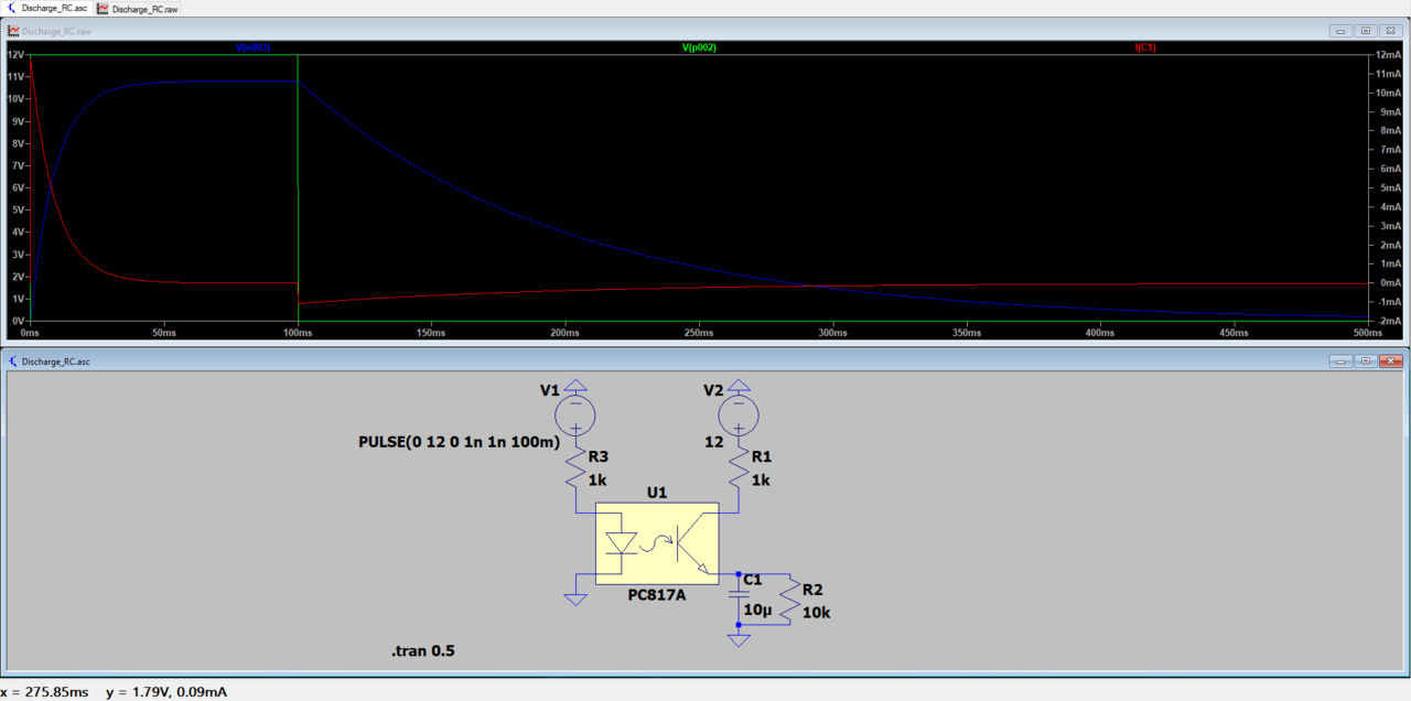
Parameters:
- Input Pulse: 100 ms
- RC Capacitor: 10 uF
- Input Resistor: 1k
This simulation shows a best case scenario. The output voltage is >1.8 V for ~250 ms for an input charging pulse of 100 ms.
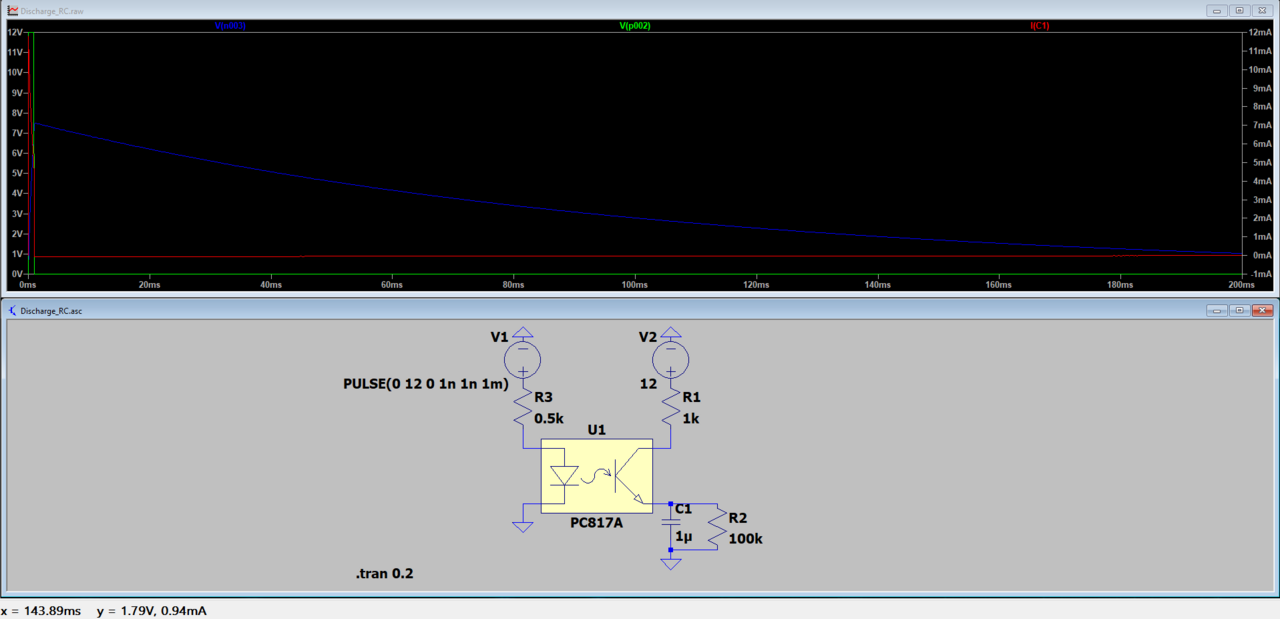
Note that my cursor was at the 1.8 V crossing for all screenshots, and you can see coordinates in the bottom left.
Simulation 3
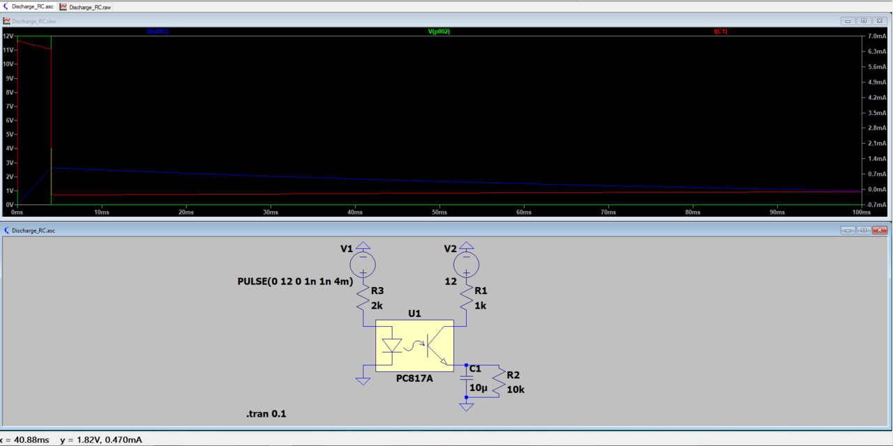
Parameters:
- Input Pulse: 4 ms
- RC Capacitor: 10 uF
- Input Resistor: 2k
My next idea was to test if CTR < 100%. I did this by putting a 2k resistor on the input and keeping the 1k resistor on the output of the optocoupler. Now, the NPN will deliver 12V/2k = 6 mA, while the resistor is trying to pull 12V/1k = 12 mA.
We see that the current is limited to a little over 6 mA, as expected.
This results in a minimum pulse length of 4 ms required to latch the relay, which is just on the edge of our requirement of 5ms latching the relay (as discussed in previous updates).
Simulation 4
Parameters:
- Input Pulse: 100 ms
- RC Capacitor: 1 uF
- Input Resistor: 0.5k
- Low-side RC circuit resistor: 100k
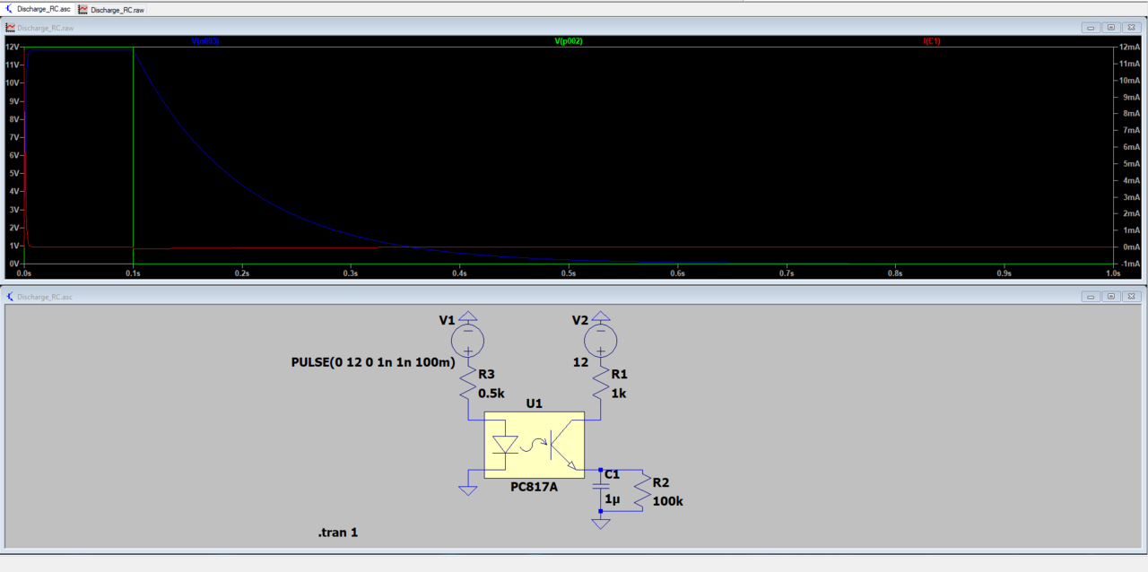
I decided to lower the capacitor to 1 uF so that it would be charged faster. Also, to ensure optimal CTR, I lowered the input resistor to 500 ohms.
I kept the high-side resistor the same, so the charging time constant is now 10x lower. I made the low-side resistor of the RC circuit 100k instead of 10k, so its time constant is equal.
This results in a much faster charging time. Notice the almost instant charging pulse on the left of the graph.
Simulation 5
Parameters:
- Input Pulse: 1 ms
- RC Capacitor: 1 uF
- Input Resistor: 0.5k
- Low-side RC circuit resistor: 100k
Next I tested the 1 uF RC circuit in a worst case scenario of a 1 ms charging pulse.
Notice that even with the 1 ms charging pulse the pulse is extended to ~130 ms!
Aarjav Jain (3h)
@Christopher Kalitin : Suppose the current components you have chosen do not meet the 5ms charging time requirement. Then can you confirm that you would only need to swap out resistors and caps to find a combination that achieves the 5ms requirement? Or would we be in a situation where the board needs to be reprinted because the circuitry may completely not work (new IC needed)?
Same logic goes for all other uses of the Optocoupler.
Christopher Kalitin (1h)
Yes, it’s all just dependent on component value choice.
There are 3 things to control for:
LED input current (input resistor)
Charging time constant (output high side resistor and capacitor)
Discharge time constant (output low side resistor and capacitor)
Unless something is fundamentally wrong with the circuit (unlikely given the LTSpice sim worked), we’ll be able to adjust components in case the current combination doesn’t work.
My concern after talking to Saman was that a low side resistor is a topology that won’t work and can’t be fixed by changing the resistor value, and the sim in the previous update confirmed this isn’t the case. The topology is fine, just resistor values have to be chosen carefully.
Previous update:
https://ubcsolar26.monday.com/boards/9702086049/pulses/18080991742/posts/4906276781